

Access VFAB

Introducing
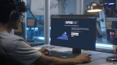
The Virtual Fabrication Access Bridge (VFAB)
Powered by VAST
The Virginia Alliance for Semiconductor Technology (VAST) brings together leading research facilities across Virginia to support cutting-edge research and development in semiconductor technology, microfabrication, nanotechnology, and biomanufacturing. VFAB highlights the combined capabilities of the participating institutions, providing a comprehensive overview of the advanced tools and resources available to researchers and industry partners. Our streamlined system allows you to conveniently schedule time in our cutting-edge semiconductor fabrication and characterization labs.
Currently, the system is only available to faculty, lab admin and students. We will be opening it up to industry soon. For more information about VFAB. please contact us: info@vast-alliance.org
The University of Virginia Innovations in Fabrication (IFAB) facility is situated within the School of Engineering and Applied Science, fostering collaboration across UVA's grounds, particularly between the School of Engineering and the College of Arts and Sciences. IFAB is a comprehensive, multifunctional facility that supports cutting-edge research in microsystems, biomanufacturing, and scalable microfabrication. This facility is designed to be an integrated, cost-share space that welcomes both UVA-affiliated and external users. It enables a broad spectrum of research endeavors, including terahertz, infrared, and photonics detectors and circuits, microfluidics, solar cells, multifunctional materials, biomanufacturing, nanobiology, soft materials, gene transfer, tissue engineering, and more.
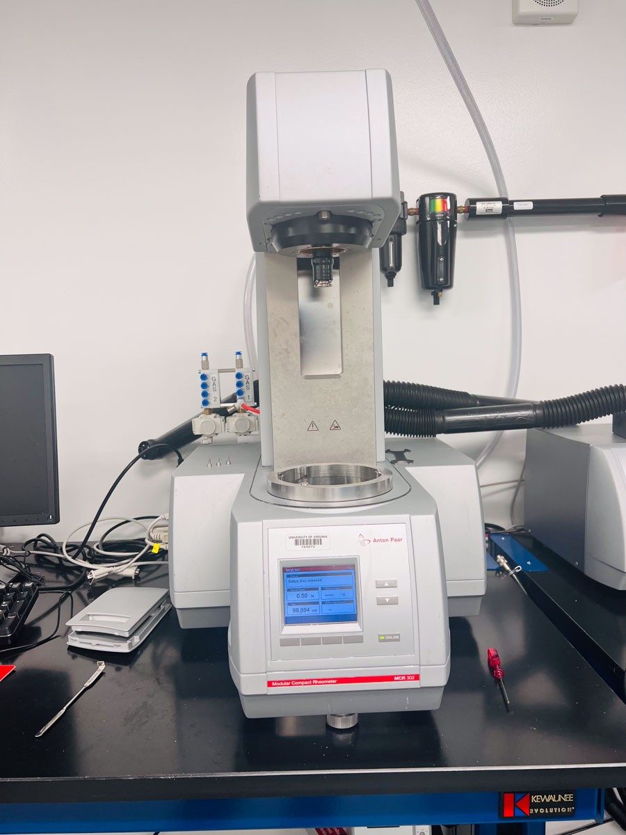
A remarkable feature of the IFAB is its state-of-the-art equipment, backed by a recent $30 million investment in infrastructure, providing a 17,500 square foot space dedicated to interdisciplinary research and transformative collaborations across and beyond the UVA community. The facility hosts an array of advanced tools, such as SUSS MABA6 Gen4Pro Mask and Bond Aligner, RAITH-150TWO E-beam Direct Write, Microwriter ML3 Laser Direct Write, and Zeiss Gemini 560 FESEM with EDS, among many others, offering highly specialized capabilities for research in the fields of microsystems, nanotechnology, biomanufacturing, and more.
IFAB is a fully open-access facility designed to catalyze collaborations both within UVA and with external entities. It provides users with a range of advanced equipment for microfabrication, nanotechnology, and biomanufacturing research. Whether you're engaged in cutting-edge nanomedicine, terahertz research, gene therapy, or tissue engineering, the IFAB provides a well-equipped space to pursue groundbreaking innovations.
UVA's Nanoscale Materials Characterization Facility (NMCF) is pleased to partner with leading industries in Virginia, providing metallurgical preparation and processing, as well as analytical services in electron microscopy, imaging, X-ray diffraction and analysis, quantitative surface composition, focused ion-beam etching, and surface chemistry. THE NMCF has instrumentation for evaluating processes and/or failure analysis thru SEM and /or TEM examination. Using imaging and EDS/EELS for characterization of the material. Below I have listed the rooms square footage and the overall space for the NMCF.
- NMCF total square footage = 5824
- XRD lab JH 108 = 332
- XRD and XRF room JH 112 = 332
- Sample cut/polish and mounting JH 129 = 378
- Sample prep Wet (etching, electropolishing, and thinning) JH131 front half = 190
- Sample prep dry (dimpling, sputter coating, Ion polishing/milling, and plasma cleaning) Back half of JH 131 = 190
- Tabletop Sem and Digital Microscope JH 139 = 296
- Conference room JH 141 (6 chairs, large table, and large screen to display from laptop) = 178
- Raman/AFM room JH 142 = 175
- XPS room JH 148 = 232
- Titan 80-300 room JH 158 = 253
- FTIR, Microhardness, Rockwell hardness room JH 162= 166
- Jesser Hall Offices for Cathy, Diane and Joe JH (149, 103, 109) = 147, 148, 140
- Themis Z HR STEM/TEM room WH B013 and B011) = 835
- Precision polishing in front half of WH B011 = 103
- Quanta 650 FEGSEM room WH B003 = 276
- Helios UC G4 Dual Beam FIB (back half of WH B001) = 294
- White light Profilometer Zygo (front half of WH B001) = 315
- Office space in Wilsdorf Hall B018 (Richard and Helge) = 196
- Helios UCG4 Dual Beam FIB - cross section areas of interest, deposit conductive material for adding connections and TEM-Lift out for TEM evaluation – perform EDS and SEM evaluation
- Titan 80-300 and Themis Z for TEM/STEM evaluation (brightfield and darkfield) (EDS, EELS, and diffraction)
- Quanta 650 for SEM evaluation and EDS
The Micron Center was created in 2006 with a donation from Micron Technologies and additional funding from the Department of Electrical and Computer Engineering. The 1800 sqft. facility is located on the 6th floor of Whittemore Hall and houses a large collection of Semiconductor and MEMS processing equipment. In addition to the clean room in W636, there are two other labs housing an array of characterization equipment in W617, along with wet processing, furnaces, sputtering and dicing capabilties in W633. The facilities are open to all university departments, in additon to users from other univsersities and surrounding companies.
Facility Details:
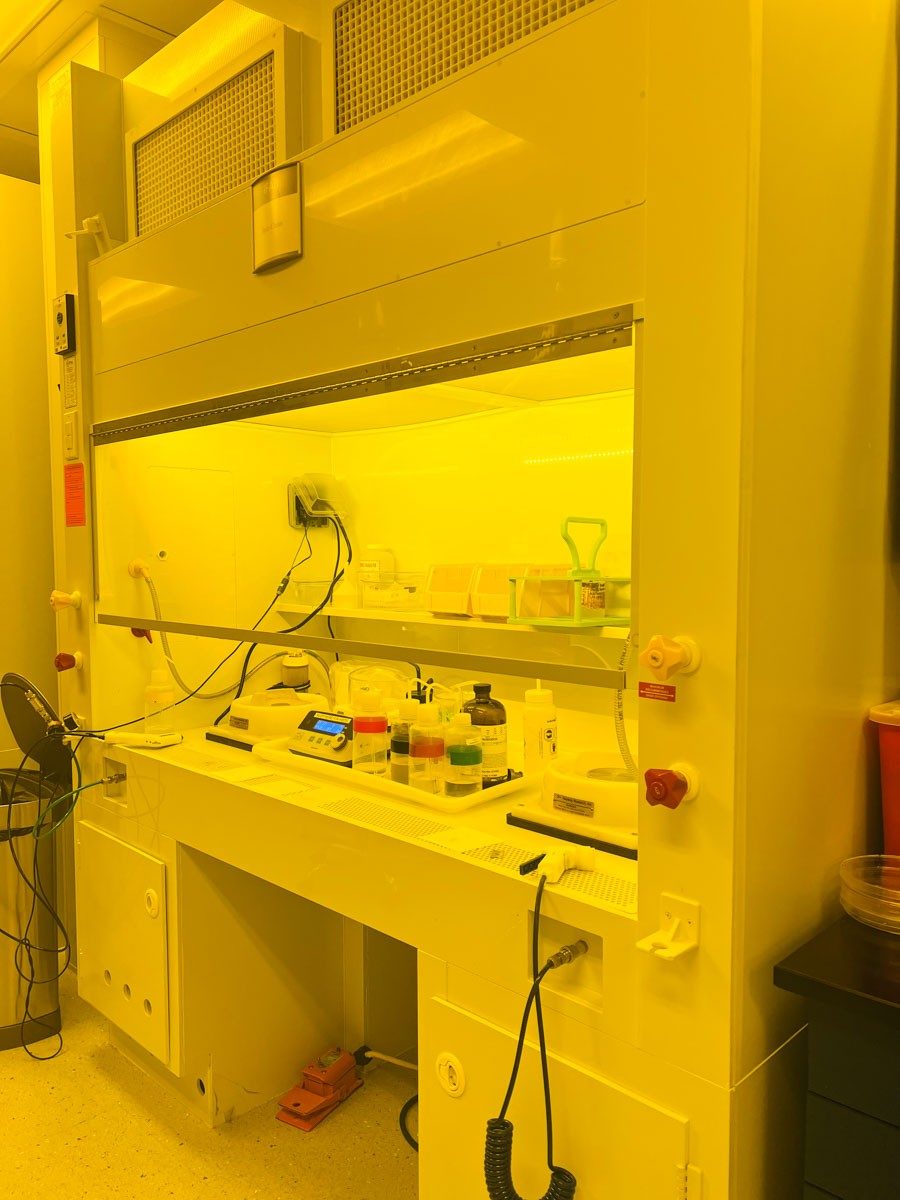
Clean Room - ~1800ft2 includes 3 wet bench areas, one for solvent/develop, one for acid/base chemical use and a third for dispensing and baking photoresist. The rest of the lab supports the majority of the process tools like photolithography, PEALD, ICP etching, PVD, and general metrology.
Whittemore 633 – ~1000ft2 Non clean room area with 4 exhaust hood for electro/electroless plating, dicing, and chemical work. Also includes Dicing, Sputtering, Rapid Thermal Annealing, and High Temp Vacuum Furnace
Whittemore 617 – ~800ft2 Characterization lab incorporating the majority of our measurement systems
a.) Bruker Dimension Icon AFM
b.) Woollam VASE
c.) Shimadzu Spectrophotometer
d.) Keithley 4200ASCS semiconductor analyzer
e.) Panalytical HRXRD
f.) Accent Electrical Chemical Profiler (IV/CV)
g.) Crosslight Software for photonic device simulation
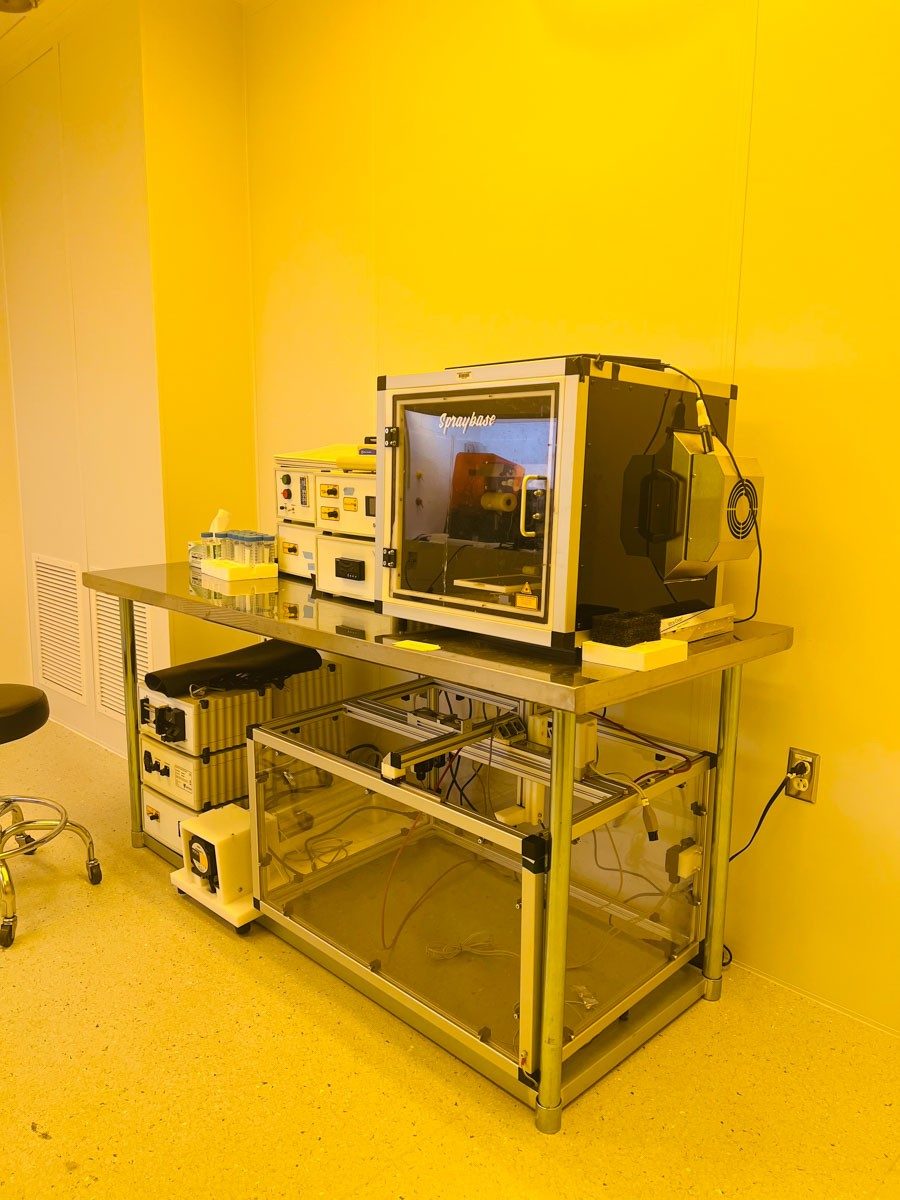
The CPES Packaging and Integration Laboratory was established to create and evaluate the design and manufacture of high-density power electronics modules, and provide the state-of-the-art electronic packaging manufacturing equipment. For substrate fabrication and patterning, the lab has the capability to produce FR4, direct bonded copper, and thick film hybrid substrates; to perform metallization using RF sputtering thin film deposition and electro(less) plating; and to develop substrate patterns by laser ablation machining and chemical metal etching. For bonding, the lab has the ability to mount bare die and surface mount components using high precision pick-n-place machine, solder reflow belt furnace, convection reflow oven, and vacuum solder reflow. Silver sintering, a high-performance bonding alternative to solder, can also be performed in the lab. Pressure-less silver sintering is performed using a manual stencil printer and programmable hotplate. Pressure-assisted sintering is performed using a hydraulic hot press. For the interconnects, the lab has wire bonding machines providing interconnect options of heavy aluminum wire bonding, gold wire ball bonding, and aluminum and gold ribbon bonding. For characterizing the bond quality, the lab features a bond tester with up to 200 kgf for shear and 100 kgf for pull. This tester is used to determine the bonding strength of wire bonds, soldered bonds, sintered bonds, and more. For encapsulating, the lab features a vacuum chamber and box furnace (up to 1100 °C) that are used for degassing and curing encapsulants. For creating module housing, fabrication jigs, and test fixtures, the lab has a 3D printer with 50-µm resolution. To evaluate the reliability of the developed modules, the lab features multiple Tenney environmental chambers with a temperature range of –55 °C to 200 °C. The lab also has a Phase 12B thermal analyzer for transient thermal impedance measurements and power cycling, and a flip-chip die bonder.
The C. Kenneth and Dianne Harris Wright Virginia Microelectronics Center (VMC) is housed in the College of Engineering (West Hall) on VCU’s Monroe Park Campus. The VMC is a shared research center providing principal investigators, students and industrial researchers training, access and technical support for their project tasks. The VMC includes more than 8,000 square feet of Class-100 and Class-1000 cleanroom space and a suite of micro- and nano-fabrication state-of-the-art tools. The bay and chase cleanroom facility is divided into three main sections: lithography, etching and deposition and sample prep. Each of these sections includes specialty equipment that provides manufacturing capabilities for researchers across many research domains. There are additional spaces connected to the VMC that are used for equipment modifications, training, process monitoring, and additional process-related tasks. All equipment and cleanroom space is maintained by expert staff. Adjacent to the VMC is the Nanomaterials Core Characterization Facility (NCC), which includes additional equipment that complements VMC’s operation.
The VMC facility offers a set of micro- nanofabrication tools which allow users to fabricate prototype device structures with dimensions down to 10 nm using photo- and/or e-beam lithography, insulator deposition, wet or dry etching, and metal thermal evaporation and/or RF sputtering.
The VMC includes more than 8,000 square feet of Class-100 and Class-1000 cleanroom space and a suite of micro- and nano-fabrication state-of-the-art tools. The majority of the auxiliary equipment (pumps, chillers, gas and chilled water delivery infrastructure are located in the chase areas separated from the cleanroom.
The bay and chase cleanroom facility are divided into three main sections: lithography, etching and deposition and sample prep. Each of these sections includes specialty equipment that provides manufacturing capabilities for researchers across many research domains. Metrology equipment are mostly located in the deposition and sample prep area.
VMC offers capabilities to produce individual devices. The major micro- nanofabrication tools available at VMC are:
- Electron-beam lithography: Raith Voyager tool with 10 nm spatial resolution.
- Photolithography: Karl Suss Microtec MJB4 Mask Aligner with 0.5 µm resolution.
- Direct photolithography: Heidelberg µMLA Maskless aligner with 0.6 µm. The tool capable of both photolithography on samples varying in size from 10x10 mm to 125 x 125 mm and generation of photomasks.
- Mask maker: Heidelberg µPG101.
- E-beam and thermal metal deposition.
- Magnetron sputtering: ATC Orion 5 UHV system with load lock. 5 sputtering guns, 4 RF and 1 DC.
- Bruce furnace for diffusion doping and silicon dioxide formation.
- Atomic layer deposition: Cambridge/Veeco Savanah tool, SiO2, HfO2, Al2O3.
- Wire bonder.
New tools are in the process of installation:
- Oxford Plasma Pro 100 Estrelas deep reactive ion etching system (DRIE) capable of both Bosch process and cryogenic RIE.
- AJA physical vapor deposition system (e-beam, high and low temperature evaporation) with load lock.
Auxiliary equipment
- Wet benches with photoresists spinners and hot plate.
- Plasma etch for photoresist stripping.
- QL vacuum furnace.
Metrology equipment
- Nikon Eclipse LV100 microscope.
- Hitachi TM3000 tabletop scanning electron microscope.
- Veeco Dektak 150 surface profilometer.
- Filmetrics F40-UV thin film analyzer for measuring thickness of dielectric and thin metal films.
The Micron-NSU Nanofabrication Cleanroom is a 6, 000 square foot facility housed in the Marie V. McDemmond Center for Applied Research (MCAR) building. It is a Class 100/Class 1 000(ISO Class 5/Class 6) user facility that provides unique processing capabilities not only to NSU researchers, but also to researchers around Hampton Roads and beyond. This cleanroom is a world-class facility that engages teams of NSU researchers in partnership with private industry, government laboratories, and other university investigators in the production of microelectronics, optoelectronics and medical devices on the micro and nano-scale.
This Cleanroom facility is an incubator for the creation of entrepreneurial enterprises that support economic strength in the Hampton Roads Community and world leadership in critical technologies for the United States.
The Micron-NSU Nanofabrication Cleanroom is a shared, state-of-the-art facility that supports a broad range of nanoscale science, engineering and technology projects by providing state-of-the-art equipment and resources coupled with expert staff support and necessary training. Frontend research projects including the fields of physical sciences, material sciences, life sciences, engineering, energy and space sciences are conducted in this cleanroom environment.
Our cleanroom and analytic lab equipment:
Thin Film
- Thermal Evaporator
- DC sputtering
- E-beam Evaporator
- RF sputtering
- Thermal EVA - NTE-3000
- Rapid Thermal Processor - RTP-600S
- Tube Furnace No. 1
- Tube Furnace No. 2
- PECVD - Vision 310
Photo
- Furnace Lindberg/Blue M(Box Type)
- Contact Mask Aligner - OAI 800
- Contact Mask Aligner - Karl Suss MJB4
- Cee 200CB Coat-Bake System No1
- Cee 200CB Coat-Bake System No2
- KW-4L Spin Coater
- Microscope System
Plasma Etching
- RIE - Phantom RIE
- RIE/ICP - Minilock Phantom RIE ICP
Inspection
- Profilometer - KLA Tencor P-16+
Characterization
- Ellipsometer
- SEM
- TEM
Back-end
- Wire Bonder
- Lapping Machine
Mason’s Nanofabrication Facility (NFF) serves as a core laboratory to conduct innovative research and development on the micro- and nano- scale. It is also a resource for providing hands-on workforce training to ensure we have a diverse, skilled workforce equipped to meet industry demand. The NFF is available to Mason faculty, staff, and students as well as external partners from academia, government, and industry.
The 1,946 Nanofabrication facility includes a class 1000 clean room and class 100,000 characterization lab.
The characterization lab is currently equipped with:
- Kloe Dilase250 Laser lithography system
- OLS40 Olympus confocal laser microscope
- Anton Parr Autoabsorb
- XRD MiniFlex 6Gr
The following tools are on-site and awaiting install:
- Temescal FC-2000 Electron-Beam Evaporator model
- Suss MA6 Mask aligner
Additional tools are being finalized for purchase with finding from a recently awarded GO Virginia grant.
The Nanofabrication Facility is situated in the Institute for Advanced Biomedical Research building, a 75,000 square-foot research facility at George Mason University’s SciTech campus (Manassas, VA). The building is occupied by a multidisciplinary team of biochemists, bioengineers, systems biologists, and mechanical engineers. The building is outfitted with dedicated cell culture labs, major instrumentation labs, imaging lab, radioactive lab, and chemistry intensive lab with 9 chemical fume hood. The facility has available drop in offices and 3 small conference rooms.
Once equipped, the nanofabrication facility will be established as a core with internal and external rates to promote usage by internal and external entities. The nanofabrication lab manager will develop the policy for whether this will be restricted to assisted work conducted by Nanofabrication laboratory technicians or if the laboratory will be opened to interested parties who would like to work independently in the laboratory.
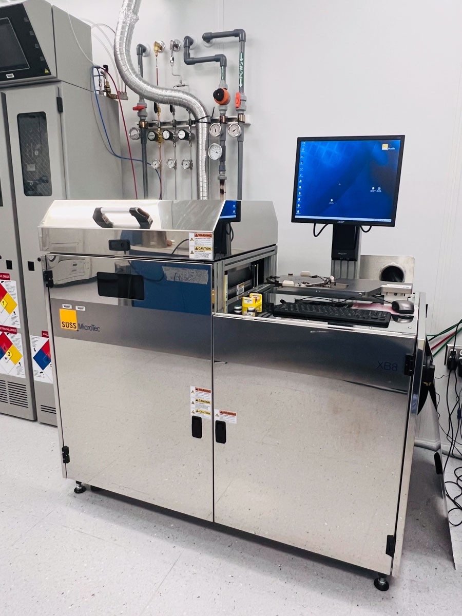
- SUSS MABA6 Gen4Pro Mask and Bond Aligner: Precision tool for front and backside alignment with UV exposure options (UV250, UV300, UV400), supporting small samples and wafers up to 4". Equipped with options for soft, hard, and vacuum contact.
- Suss MJB4 Mask Aligner: UV (360nm) mask aligner for topside alignment, especially for thick resists like SU8 and KMPR. Supports various exposure modes.
- EVG620 (2002) Aligner: i-line (320nm) mask aligner for topside alignment with reduced backside alignment capabilities.
- RAITH-150TWO E-beam Direct Write: E-beam lithography with ~8nm resolution, beam energies from 20 eV to 30 keV, 20 MHz pattern generator, and automated height sensing.
- Microwriter ML3 Laser Direct Write: Laser system for rapid prototyping with a maximum writing area of 195mm x 195mm and wafer sizes up to 230mm x 230mm.
- Karl Suss MA-6/BA-6 Mask Aligner: High-resolution photolithography for substrates up to 6 inches, supporting both frontside and backside alignment.
- OAI 800E Front and Backside Semiautomatic Mask Aligner: Semi-automatic aligner for frontside and backside photolithography with high precision.
- SF100 Maskless Photolithography System: High-resolution maskless lithography system capable of direct patterning with a resolution of 2 µm.
- Heidelberg Instruments μMLA Maskless Alignment System: Direct writing of design data into photoresist for high-precision fabrication, handling substrates from 5x5 mm² to 6” x 6”.
- Heidelberg Instruments uMLA Maskless Aligner: Capable of exposing structures down to 600 nm.
- Heidelberg Instruments uPG 101 Mask Maker: Minimum feature size of 0.6 μm, maximum substrate size of 6" x 6".
- Raith Voyager E-beam Lithography System: Up to 50 kV accelerating voltage, sub-8nm features, and 500 µm write field size.
- JEOL JBX-8100FS Electron Beam Lithography System: Ultrahigh resolution of 2 nm for intricate nanostructures.
E-beam Evaporators:
- CHA-Solution E-beam Evaporators (Left & Right): Six-crucible systems with ion gun cleaning, handling wafer sizes from 2" up to 4".
- Kurt J Lesker PVD-250 E-beam Evaporator: For metals and dielectrics, equipped with a Kauffman Ion Gun.
- E-beam and Thermal Deposition System: Six-crucible evaporator with ion-gun cleaning, supporting various materials.
- AJA E-beam Evaporator: Six crucibles for e-beam evaporation with thermal evaporation options.
Sputtering Systems:
- Lesker CMS-18 Magnetron Sputter: DC and RF magnetron up-sputter system with a 6-gun configuration, suitable for materials such as Ti, Au, Cr, and Ni.
- Kurt J. Lesker Company PRO Line PVD 75 Sputter System: Co-sputtering from multiple targets, supporting substrates up to 6 inches.
- Kurt J Lesker PVD-75 Sputtering System: DC and RF capabilities for various material depositions.
- AJA ATC-Orion 5 Sputtering System: DC and RF magnetron sputtering system with 5-gun confocal sputtering setup.
Chemical Vapor Deposition (CVD):
- Oxford ICP-CVD PlasmaPro 100 Cobra 300: High-quality, low-temperature deposition of Si, SiO2, and Si3N4 films.
- SPTS LPX DELTA PECVD: For SiO₂ and Si₃N₄ film depositions.
- SAMCO PECVD PD-220NL: Load-lock type PECVD system for SiO2, a:Si, and SiNx films.
Atomic Layer Deposition (ALD):
- Oxford FlexAL RPT ICP-ALD Growth: Precise thin film growth on a wide range of materials including oxides (Al₂O₃, HfO₂, TiO₂), nitrides (Si₃N₄, AlN, TiN), and metals.
- Cambridge Atomic Layer Deposition (ALD) System: For depositing thin films with atomic precision, including dielectrics like hafnium oxide and aluminum oxide.
Specialty Deposition Systems:
- 4WAVE RBTIBD: Reactive bias target ion beam deposition system for advanced materials applications.
- KJLC PVD75 DC Sputtering: For conductive materials like Si, SiO2, Ti, Au, and Ag.
- KJLC PVD75 RF Sputtering: For insulator materials, supporting various materials upon approval.
- KJCL PVD75 E-Beam Evaporation: High-energy electron beam for high deposition rates.
- KJLC PVD75 Thermal Evaporation: High uniformity system for evaporating materials onto substrates.
Reactive Ion Etching (RIE)
- SOxford Plasmalab 100 ICP-RIE (Chlorine + Fluorine): For processing small samples and wafers with various etching gases.
- SPTS LPX OMEGA ICP Etcher: High-density plasma etcher for precise, anisotropic etching of oxides, nitrides, and metals.
- Samco RIE: For precise etching of silicon dioxide, silicon nitride, and photoresist.
- Trion RIE Phantom Metal Etcher: For metal etching of 4" wafers and 5" photomasks with chlorine-based chemistries.
- Semigroup RIE: Optimized for etching with fluorine gases (SF6, CF4, CHF3).
- XeF2 Isotropic Si Etcher: Non-plasma, isotropic etching of silicon, particularly suitable for MEMS applications.
- SPTS LPX Rapier DRIE: Deep reactive ion etching system for MEMS applications and high-aspect-ratio silicon etching.
- SPTS Primaxx Uetch: Vapor-phase etching system utilizing anhydrous HF for delicate MEMS structures.
- Oxford PlasmaPro 100 Estrelas: ICP-RIE system for deep BOSCH Si etching and Cryo etch technology.
- Plasma Etch Tabletop Plasma System: O2 plasma etcher for cleaning processes.
- Trion Inductively Coupled Plasma Reactive Ion Etching (ICP-RIE): For plasma etching using fluorine and oxygen-based chemistries.
Dry Etching:
- Semigroup RIE: Optimized for etching with fluorine gases (SF6, CF4, CHF3).
- XeF2 Isotropic Si Etcher: Non-plasma, isotropic etching of silicon, particularly suitable for MEMS applications.
- SPTS LPX Rapier DRIE: Deep reactive ion etching system for MEMS applications and high-aspect-ratio silicon etching.
- SPTS Primaxx Uetch: Vapor-phase etching system utilizing anhydrous HF for delicate MEMS structures
- Oxford PlasmaPro 100 Estrelas: ICP-RIE system for deep BOSCH Si etching and Cryo etch technology.
- Plasma Etch Tabletop Plasma System: O2 plasma etcher for cleaning processes.
- Trion Inductively Coupled Plasma Reactive Ion Etching (ICP-RIE): For plasma etching using fluorine and oxygen-based chemistries
Scanning Electron Microscopy (SEM):
- Zeiss Gemini 560 FESEM with EDS: High-resolution FESEM with 0.5nm resolution at 30kV, equipped with an EDS detector for elemental analysis.
- Hitachi SU8010 FE-SEM: Cold field emission SEM with ultra-high-resolution imaging capabilities for surface analysis, ranging from 100x to 800,000x magnification.
- Phenom XLG2 SEM: High-resolution imaging and microanalysis with BEI and SEI electron imaging, also offering EDS for elemental analysis.
- Quanta 650 FEGSEM: Field-emission SEM with EDS and EBSD for crystallographic characterization and strain analysis.
- Hitachi TM3000 Tabletop SEM: Offers a resolution of 30 nm for surface characterization.
Transmission Electron Microscopy (TEM):
- Titan 80-300 TEM: Atomic-scale imaging and composition analysis with EDS, offering various imaging modes including bright-field and dark-field.
- Hitachi TEM HT7800: High-resolution TEM with multiple lens configurations, including a HR lens for high-resolution imaging.
- ThemisZ HRSTEM: Advanced STEM with integrated EDS and EELS analysis, offering unparalleled capabilities for materials characterization.
Focused Ion Beam (FIB):
- Helios G4 UC FIB: High-precision milling and electron microscopy capabilities, performing ion-beam deposition and quantitative elemental mapping with EDS.
X-ray Diffraction (XRD):
- Empyrean X-ray Diffractometer: Phase identification and quantification for crystalline powders and solids with crystallite sizes greater than 5nm. Suitable for inorganic, organometallic, and organic substances, with an optional heated stage for additional analysis.
- X'pert Pro X-ray Diffractometer: Provides X-ray diffraction measurements for a variety of crystalline materials, essential for phase identification and quantification of powders and solids.
- SmartLab X-ray Diffractometer: Ideal for GI-XRD, X-ray reflectivity, micro-diffraction, and 2-D techniques, enabling advanced materials analysis.
- Bruker D2 Phaser Diffractometer: Bench-top XRD system for measuring diffraction of samples that fluoresce under Cu X-rays, allowing for phase identification and quantification.
Spectroscopy:
- Versaprobe X-ray Photoelectron Spectrometer (XPS): Quantitative elemental and chemical analysis of material surfaces, with small-spot and large-area analyses, depth profiling, and in situ sample heating.
- HIPP-Lab XPS: Advanced surface analysis with angle-resolved XPS, valence band structure analysis, and in situ electrochemistry.
- Fourier-transform Infrared Spectroscopy (FTIR): Compound identification and molecular bonding analysis with the Bruker Invenio-S FTIR system, suitable for solids, films, and liquids.
- Epsilon III X-ray Fluorescence (XRF): Elemental analysis, contaminant detection, and material identification of solids, liquids, and powders, with high sensitivity for elements with Z > 10.
Optical and Microscopical Imaging:
- Hirox RH-8800 Optical Microscope: Nondestructive imaging, videography, and surface measurements with magnifications up to 5000x, supporting 3-D modeling and time-lapse videography.
- Renishaw InVia Raman & Bruker InnoVA AFM: Confocal Raman microscope integrated with an AFM for chemical composition analysis and topographic, nano-mechanical, and electronic property mapping. Supports Raman mapping with 1 micron spatial resolution.
- Zygo New View 7300 White Light Profilometer: Optical profilometer for determining surface topography, measuring surface roughness, and analyzing surface texture and asperity.
- Bruker Dimension Icon® AFM: Scanning probe microscope for detailed topographical, mechanical, electrical, and magnetic analysis.
- Bruker Dektak-XT Surface Profiler: Stylus-based surface profiler for measuring roughness and topography with 1mm vertical and 50mm horizontal range.
- J.A. Woollam M-2000-DI Ellipsometer: Spectroscopic ellipsometer for thin film analysis, with a wavelength range from 193nm to 1690nm, and a resolution of over 500 wavelengths.
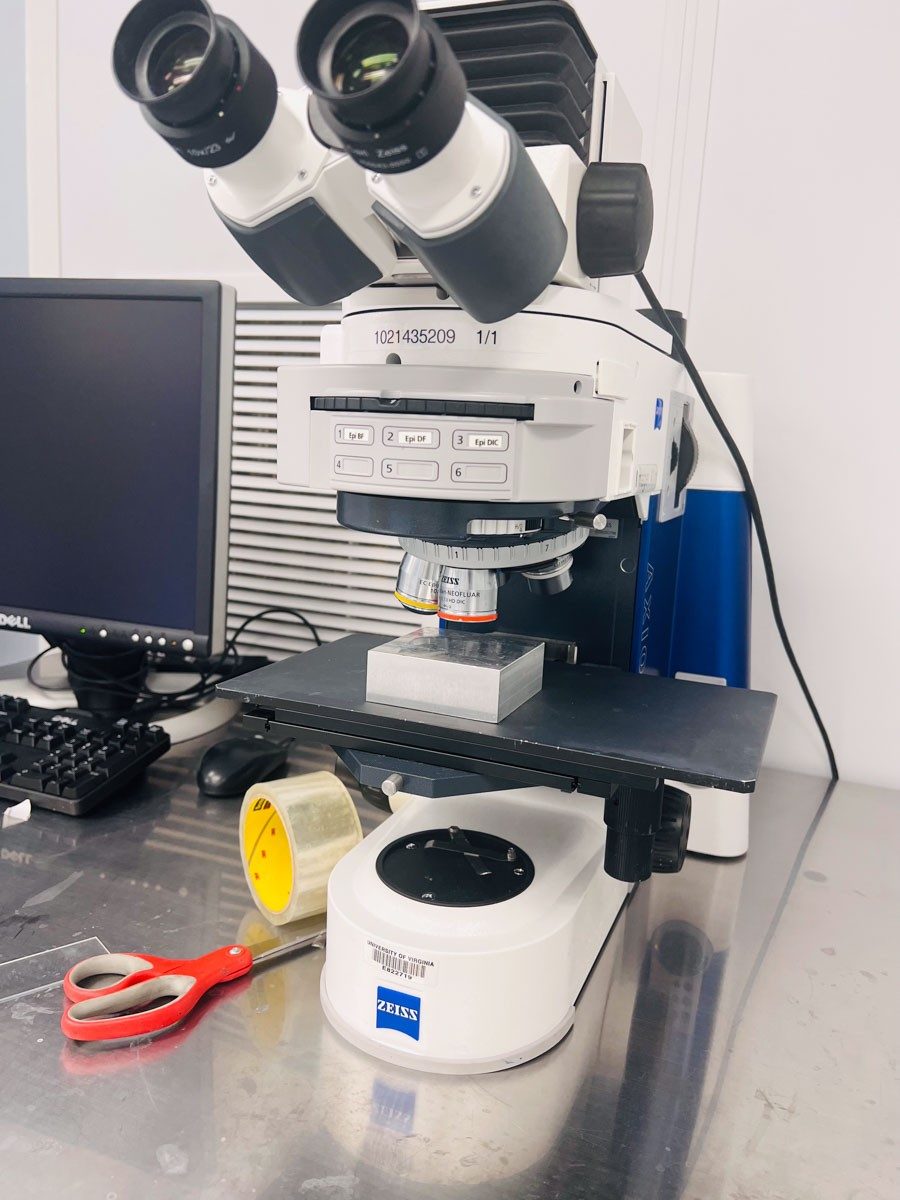
- ZEISS Axio Imager.M2m Inspection Microscope: High-resolution inspection microscope for analyzing structures in detail.
- Olympus OLS4000 Laser Microscope: Non-contact optical profilometer using laser scanning for detailed topographic data.
- Olympus MX63 Inspection Microscope: High-resolution imaging for microfabrication projects.
- Keyence VHX 7000 Digital Microscope: A high-resolution digital microscope offering magnifications up to 6000x.
- Shimadzu Spectrophotometer UV-3101 UV-VIS-NIR: A spectrophotometer for detailed optical characterization of materials.
3D Bioprinting
- CellInk BioX Bioprinter
- RegenHu 3D Printer
Live Cell Imaging
- EVOS M7000 Live Cell Imaging Microscope
Cell and Sample Preparation
- Normoxia and Hypoxia Rooms
- Cell Culture Incubators
Substrate & Die Processing
- Laser Ablation Machining
- Chemical Metal Etching
- Screen Printing
Mounting & Bonding
- Silver Sintering Technology
- Solder Reflow Belt Furnace
- Convection Reflow Oven
- Wire Bonding Machines
Device Attachment & Reliability Testing
- Multi-Purpose Bond Testing Equipment
- Die Attach Systems
Module-Level Testing & Evaluation
- Thermal Analysis
- Electrical & Reliability Performance Testing
Specialized Semiconductor Packaging Equipment
- Keyence Digital Microscope
- Keyence Optical Profilometer
- Kewaunee Fume Hood
- Form Labs 3D Printer
- DDM Novastar Reflow Belt
Lapping and Polishing
- Logitech PM5 Lapping Machine
Dicing and Bonding
- ADT 7122 Dicing Saw
- Disco DAD3220 Dicing Saw
- Kulicke & Soffa I 5000 Wire Bonder
Thermal Processing
- EMS Tabletop Thermal Oxidation Furnace
- EMS Tabletop Solid Source Doping Furnace
- Allwin AW-610 M Rapid Thermal Processor
- High Temperature Vacuum Tube Furnace
- Vulcan Box Furnace
- Torrey Pines Hot Plate
Cleaning and Preparation
- Ion Wave 10 Plasma Asher
- HMDS Vapor Prime Oven
- Chemical & Wet Processing Hoods
- Plating Stations
- QL Vacuum Oven
- Cascade Tek Vacuum Oven
Electrical Characterization
- Keithley 4200A Semiconductor Analyzer
- Signatone 4-pt Probe/Keithley 2400
- Keithley Digital Multimeter
- Agilent 317B Curve Tracer
Thermal and Mechanical Testing
- Analysis Tech Thermal Analyzer
- Xdry 302 Dry Box
- TPT Wire Bonder
- Carver Hydraulic Press
- XYZTec Die Shear Test System
- Universal Laser System
- BOFA Fume Extractor
- Flir Thermal Camera
- E75 Thermal Camera
- Tenney TPS Thermal Test Chamber
Our Impact
Fostering Innovation and Excellence
The VAST facilities collectively offer a robust platform for interdisciplinary research and innovation. By leveraging the advanced tools and resources available across these institutions, researchers and industry partners can drive advancements in semiconductor technology, nanotechnology, biomanufacturing, and beyond. The collaborative environment fostered by VAST ensures that users have access to the expertise and equipment necessary to achieve groundbreaking scientific and technological breakthroughs.
Federating more than 35,000 sq. ft of shared semiconductor fabrication facilities.

Serving more than 150 faculty research groups & training more than 600 students.

Federating more than 30,000 sq. ft of shared material metrology & semiconductor packaging facilities.

Will upskill 300 veterans & adult learners annually through the Fast Track to Semiconductor Careers Certificate Program.
Need Help Navigating the Tool?
VAST has put together some educational materials to get your acclimated to our VFAB. Choose the topic that interests you below:
Access the VFAB Manual
Navigating the Dashboard
Creating your Account
Equipment Overview Videos
